

TL;DR

- Record Capital Commitment: Micron's cumulative investment in Taiwan has exceeded NT$1.6 trillion, with investments over the past four years matching its total across the preceding 25 years.
- Four-Site Manufacturing Push: Micron is actively scaling operations across Taichung (HBM packaging), Tongluo (front-end P5 fab), Taoyuan (Fab 11E for EUV/High-NA EUV), and Tainan (cleanroom testing conversion).
- Nanya Adds Pingtung Site: Taiwan's National Science and Technology Council (NSTC) has approved Nanya Technology's plan to develop advanced 3D wafer packaging and testing using through-silicon via (TSV) technology in Pingtung.
- Sector-Wide Expansion: Combined additional capital expenditures from Micron, Nanya Technology, and Winbond are projected to approach NT$200 billion.
Global memory manufacturers are significantly deepening their manufacturing footprints in Taiwan as demand surges for advanced dynamic random-access memory (DRAM) and artificial intelligence infrastructure. According to a report by Economic Daily News, Micron Taiwan Chairman Donghui Lu confirmed that the company is deploying its most advanced memory manufacturing processes to Taiwan, backed by multi-facility developments underway in Taichung, Tongluo, Taoyuan, and Tainan.
At the same time, Taiwan's National Science and Technology Council (NSTC) has approved a major initiative by domestic memory maker Nanya Technology to establish operations at the Pingtung Science Park, Central News Agency reported. Together with ongoing expansions by Winbond in Kaohsiung, the collective additional capital outlays across the three memory producers are anticipated to approach NT$200 billion.
Micron Expands Advanced DRAM and HBM Footprint Across Four Sites
Micron is undertaking the broadest expansion among the memory makers, covering both front-end wafer fabrication and back-end advanced packaging. As of June, Micron had invested more than NT$1.6 trillion in Taiwan, with tens of billions more expected. The scale of this recent deployment is unprecedented for the company: Economic Daily News reported that Micron's investments in Taiwan over the last four years have already equaled its aggregate investment from the previous 25 years.
A cornerstone of this roadmap is the introduction of Micron's cutting-edge 1γ (1-gamma) DRAM process to Taiwan, marking the company's first DRAM node to leverage extreme ultraviolet (EUV) lithography.
Taichung: Scaling High Bandwidth Memory (HBM) Packaging
Taichung serves as Micron's primary manufacturing stronghold in Taiwan. In response to tight capacity across existing advanced packaging lines, the company initiated the conversion of a conventional facility into a dedicated second advanced packaging plant in 2025. According to Commercial Times, this facility is scheduled to begin commercial operations in mid-October 2026, primarily providing dedicated capacity for High Bandwidth Memory (HBM) packaging.
Tongluo: Accelerating P5 Fab Operations
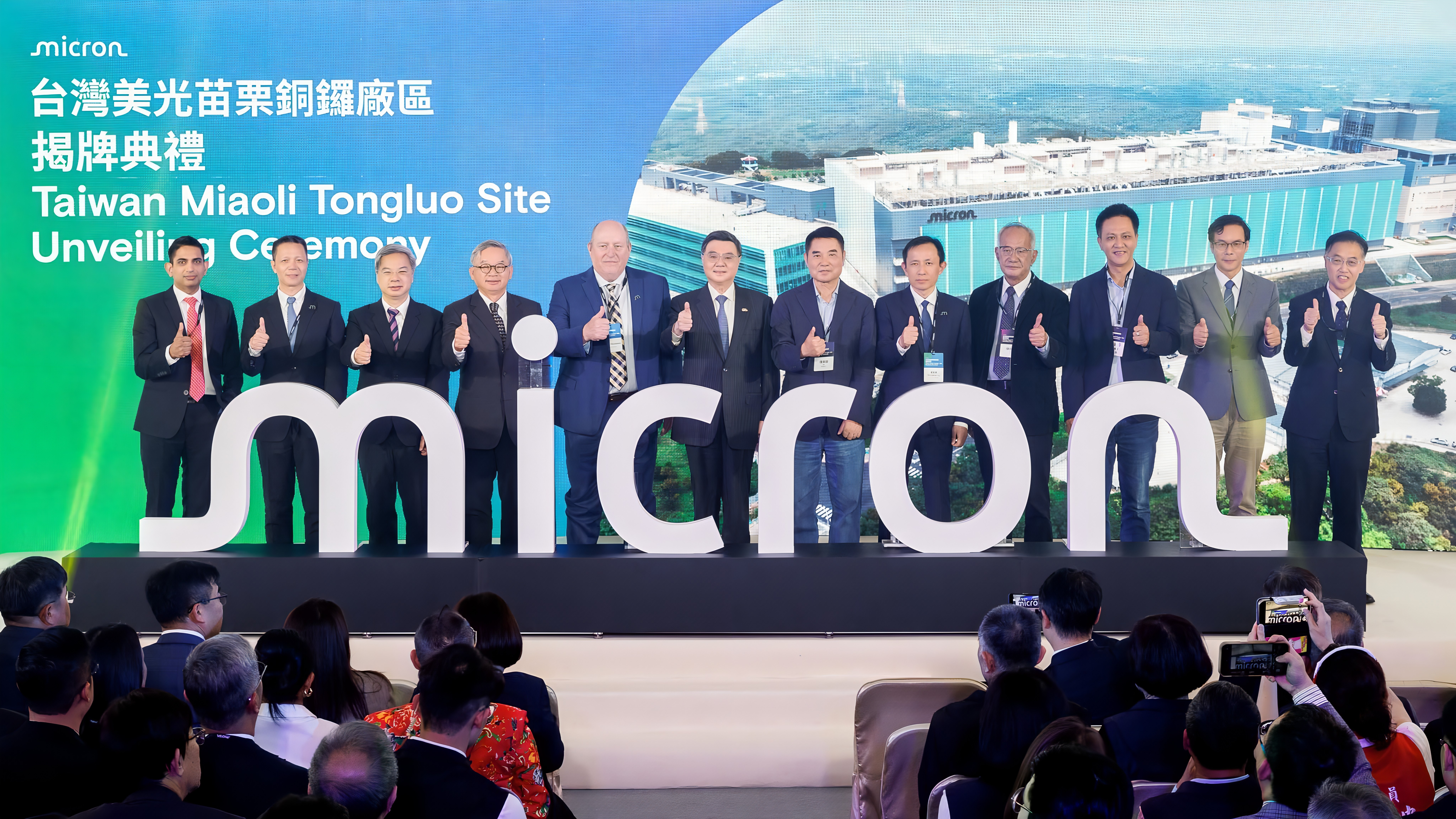
In Tongluo, Micron is progressing with front-end capacity at the P5 wafer fab, which it acquired from Powerchip Semiconductor Manufacturing Corp. (PSMC) earlier this year. More than 100 pieces of manufacturing equipment have already been transferred into the facility, and preliminary construction on a second facility has commenced, Economic Daily News noted. Central News Agency reported that Micron targets the second half of 2027 to launch the first phase of production at the expanded Tongluo facility.
Taoyuan: Constructing Fab 11E for EUV and High-NA Lithography
At its Taoyuan campus, Micron is constructing Fab 11E. The facility is specifically engineered to accommodate high-precision EUV lithography equipment, and its structural design incorporates specifications required for future High-NA (High Numerical Aperture) EUV tools. According to Economic Daily News, Fab 11E is slated to come online around 2028.
Tainan: Converting Industrial Space into Testing Cleanrooms
In Tainan, Micron is repurposing a former display panel facility acquired from AUO into a specialized semiconductor site. Micron Taiwan Chairman Donghui Lu stated that engineers have converted an 11-meter-high warehouse structure into a three-story cleanroom facility. Equipment installation began in early September 2026, with the site designated to focus primarily on front-end wafer testing operations.
Nanya Technology Advances 3D Wafer Packaging in Pingtung
Alongside Micron's expansion, domestic DRAM manufacturer Nanya Technology is expanding its presence into southern Taiwan. Central News Agency reported that the NSTC approved Nanya's project at Pingtung Science Park, where the company plans to establish research, development, and production lines for advanced 3D wafer packaging and testing.
Nanya's technical focus at Pingtung centers on through-silicon via (TSV) architecture and wafer-stacking technologies. While Nanya Technology has not officially disclosed the total financial commitment for the Pingtung development, industry estimates cited by Economic Daily News indicate that constructing and equipping a new semiconductor fab requires at least NT$100 billion.
Industry Investment Approaches NT$200 Billion
The aggressive capital spending by Micron and Nanya coincides with ongoing expansion initiatives by Winbond Electronics in Kaohsiung. Combined, the additional investments across these three memory fabricators are projected to near NT$200 billion, underscoring Taiwan's central position in the global memory supply chain.
Key Technologies Driving Taiwan's Memory Expansion
The latest wave of capital deployment centers on several critical semiconductor manufacturing and packaging technologies:
- High Bandwidth Memory (HBM): A high-performance memory architecture where DRAM dies are vertically stacked and interconnected, offering significantly higher data bandwidth and energy efficiency essential for AI accelerators.
- Extreme Ultraviolet (EUV) & High-NA Lithography: Optical printing systems utilizing short-wavelength light to pattern sub-microscopic circuits on silicon wafers. Next-generation High-NA EUV optics provide even finer resolution for future advanced process nodes.
- Through-Silicon Via (TSV) & Wafer Stacking: Vertical electrical pathways that pass completely through silicon dies, enabling tight, three-dimensional chip stacking and ultra-low-latency data transfer between layers.
- Front-End vs. Back-End Processing: Front-end fabrication involves printing electronic circuits onto raw silicon wafers, whereas back-end operations encompass cutting, advanced packaging, and testing to produce completed modules.
Why This Investment Wave Matters
The scale of memory investments reflects the shifting technological requirements of modern computing workloads. As artificial intelligence models demand exponentially higher memory bandwidth and density, memory manufacturers are moving beyond standard planar DRAM architectures to integrated 3D stacking and advanced lithography. By establishing front-end EUV fabs and specialized HBM packaging lines within Taiwan, chipmakers are streamlining manufacturing logistics and tightly coupling memory production with the broader regional semiconductor ecosystem.
Frequently Asked Questions
How much has Micron invested in Taiwan?
Micron's cumulative investment in Taiwan exceeded NT$1.6 trillion as of June, with tens of billions more expected. According to Economic Daily News, the company's capital expenditures in Taiwan over the last four years have matched the cumulative total from the prior roughly 25 years.
What operations are included in Micron's four Taiwan expansion sites?
Micron's four active expansion sites include:
- Taichung: A second advanced packaging facility scheduled to open in mid-October 2026, dedicated primarily to HBM capacity expansion.
- Tongluo: Expansion of the P5 fab acquired from PSMC, with initial production targeted for the second half of 2027.
- Taoyuan: Construction of Fab 11E, designed for EUV and future High-NA EUV equipment, projected to begin operations around 2028.
- Tainan: A converted former AUO display facility featuring a newly built three-story cleanroom focused on front-end wafer testing.
What is Nanya Technology building in Pingtung Science Park?
Nanya Technology received approval from Taiwan's National Science and Technology Council to set up operations in Pingtung Science Park, where it intends to develop advanced 3D wafer packaging and testing using through-silicon via (TSV) and wafer-stacking technologies. While Nanya has not officially disclosed the budget, industry estimates indicate a new fab requires at least NT$100 billion.
Which memory manufacturers are expanding in Taiwan?
The major memory producers actively expanding capacity in Taiwan include Micron Technology, Nanya Technology, and Winbond Electronics (which is expanding in Kaohsiung). Combined additional investments across the three companies are expected to approach NT$200 billion.


0 Comments